This page is not the official website. Generated by AI, does not constitute any advice. If needed, please click here to visit the corresponding official website.

Ganwafer – Advanced
Compound Semiconductor Wafers

A leading manufacturer and R&D center in China specializing in GaN, SiC, and III-V compound semiconductor materials. Delivering high-quality wafers and epitaxy services for power electronics, RF, optoelectronics, and advanced research.

About Ganwafer

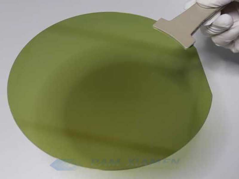
Ganwafer is a top-class enterprise integrating semiconductor crystal growth, process development, and epitaxy. As a condensed matter physics research center and a leading manufacturer of compound semiconductor materials in China, we specialize in creating cutting-edge crystal growth and epitaxy technologies.

Founded with a vision to advance next-generation semiconductor materials, Ganwafer has been at the forefront of innovation since 1990. We began with CZ silicon wafers and ingots, expanded into second-generation GaAs and InP wafers in 2004, and now lead in third-generation materials like SiC and GaN.

  • Over 30 years of semiconductor expertise
  • Specializing in GaN, SiC, and III-V materials
  • Full-service epitaxy and wafer fabrication
  • Global customer support and technical service
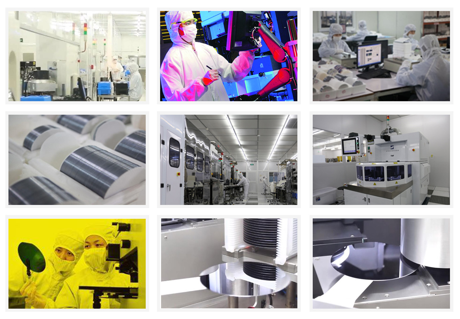
Ganwafer Laboratory

Why Choose Ganwafer?

We combine decades of research, cutting-edge technology, and customer-focused service to deliver the highest quality semiconductor materials.

Proven Quality & Reliability

Our wafers undergo rigorous testing and quality control to ensure consistency, low defect density, and optimal performance for high-power and high-frequency applications.

Advanced R&D Capabilities

With a strong technical R&D team, we continuously improve existing materials and develop next-generation solutions tailored to market demands and emerging technologies.

Customer-Centric Service

From custom epitaxy to technical support, we work closely with clients to meet specific requirements and accelerate time-to-market for innovative semiconductor devices.

Our Product Range

Comprehensive portfolio of compound semiconductor wafers and epitaxial services for research, development, and mass production.

N Type Freestanding GaN Substrate

N Type Freestanding GaN Substrate

High-quality GaN substrates with controlled n-type doping for power electronics and RF applications.

  • • Diameter: 2", 4"
  • • Doping: Si-doped
  • • Orientation: C-plane, A-plane, M-plane
  • • Low dislocation density
GaN on Silicon HEMT Wafer

GaN on Silicon HEMT Wafer

High-electron-mobility transistor (HEMT) structures on silicon for cost-effective power devices.

  • • Substrate: Si (111)
  • • Structure: AlGaN/GaN heterojunction
  • • Applications: Power amplifiers, converters
  • • Customizable threshold voltage
GaAs Wafer

GaAs Wafer

High-purity gallium arsenide wafers for optoelectronics and high-speed devices.

  • • Diameter: 2", 3", 4", 6"
  • • Doping: Semi-insulating, n-type, p-type
  • • Orientation: (100), (111)
  • • Low EL2 concentration
InP Wafer

InP Wafer

Indium phosphide substrates for high-speed communication and photonic devices.

  • • Diameter: 2", 3", 4"
  • • Doping: Fe-compensated, n-type, p-type
  • • Low dislocation density
  • • Ideal for 1.55μm lasers and detectors
Silicon Epi Wafer

Silicon Epi Wafer

Epitaxial silicon layers on CZ or FZ substrates for advanced CMOS and power devices.

  • • Diameter: 150mm, 200mm, 300mm
  • • Resistivity: 0.001–100 Ω·cm
  • • Thickness: 1–100μm
  • • Low autodoping, high uniformity
III-V Epi Wafer

III-V Epi Wafer

Custom epitaxial structures on GaAs, InP, and GaSb substrates for optoelectronics and quantum devices.

  • • MBE and MOCVD growth
  • • Quantum wells, superlattices
  • • InGaAs, InGaAsP, AlGaAs
  • • Low defect density
InGaAsP Quantum Well

InGaAsP / InP Quantum Well

1.5μm InGaAsP/InP quantum well laser structures for fiber optic communication.

  • • Emission: 1.5μm band
  • • MQW active region
  • • Low threshold current
  • • High reliability
Si-Delta Doped GaAs

Si-Delta Doped GaAs PHEMT

High-performance pseudomorphic HEMT heterostructures for millimeter-wave applications.

  • • InGaAs channel
  • • Si-delta doping
  • • High electron mobility
  • • Low noise figure
View Full Wafer List

Advanced Technology

At Ganwafer, we leverage state-of-the-art crystal growth and epitaxy techniques to deliver superior semiconductor materials.

Crystal Growth Expertise

Our expertise spans multiple crystal growth methods including HVPE for freestanding GaN, LEC and VGF for InP and GaSb, and PVT for SiC. This enables us to produce substrates with exceptional crystalline quality and low defect density.

We have continuously refined our processes since 1990, starting with CZ silicon and expanding into compound semiconductors. Our proprietary techniques ensure high yield and reproducibility across batches.

  • • Hydride Vapor Phase Epitaxy (HVPE)
  • • Liquid Encapsulated Czochralski (LEC)
  • • Vertical Gradient Freeze (VGF)
  • • Physical Vapor Transport (PVT) for SiC
  • • Molecular Beam Epitaxy (MBE)
  • • Metalorganic Chemical Vapor Deposition (MOCVD)

Epitaxy & Device Structures

Our epitaxy services cover a wide range of device structures tailored for specific applications in power, RF, and optoelectronics.

GaN HEMT Structures

AlGaN/GaN on Si, SiC, or Sapphire for high-electron-mobility transistors

LED/LD Epi Wafers

InGaN-based blue/green LEDs and InGaAsP/InP lasers at 1.3–1.55μm

Quantum Devices

Delta-doped PHEMTs, quantum wells, and superlattices

Custom Development

We collaborate with customers to develop novel material systems

Latest News & Updates

Stay informed about our latest developments, technical breakthroughs, and product launches.

April 20, 2023

GaN/Si HEMT Structure

We have optimized our GaN-on-Si HEMT structure for improved threshold voltage stability and reduced current collapse.

Read More
April 11, 2023

InSb MBE Growth

Successful growth of high-mobility InSb layers using molecular beam epitaxy for infrared detector applications.

Read More
January 29, 2023

1.5μm InGaAsP / InP Quantum Well Laser

New quantum well laser structure with low threshold current and high temperature stability.

Read More
November 15, 2022

InP / InGaAs for PIN NIR Diode

High-responsivity near-infrared photodetector structure on InP substrate.

Read More
November 4, 2022

InGaAsP Thin Film

Lattice-matched InGaAsP films for long-wavelength optoelectronic devices.

Read More
October 8, 2022

Red LED Thin Film Wafer

High-efficiency red LED structure based on AlInGaP/GaAs technology.

Read More

Contact Ganwafer

For sales inquiries, technical support, or custom wafer requests, reach out to our team.

Contact Information

Email

[email protected]

[email protected]

Address

No.77, Lingxia Nan Road, High Technology Zone, Huli, Xiamen, 361006, China

Visit our official website to submit inquiries, request quotes, or access technical documentation.

Visit Official Website

Notice for Buyers: If you are a buyer, the above information is generated by AI collection and does not constitute any advice. If necessary, please visit the corresponding official website.

For Domain Owners: If you are the domain owner and do not want to be included by fobcompany.info, please contact [email protected] via your corporate email to cancel. We will cancel your inclusion within 3 business days.

如果您是域名所有者 不想被fobcompany.info收录 请用企业邮箱联系[email protected] 取消收录 我们将在3个工作日取消您的收录

Service Request: If you are other domain and want to be included, please contact [email protected]

如果您是其他域名合作 也请联系[email protected]