This page is not the official website. Generated by AI, does not constitute any advice. If needed, please click here to visit the corresponding official website.

Professional HDI PCB Manufacturer for High-Tech Applications

Huizhou Runtek Co., Ltd. delivers high-reliability, high-tech PCB solutions with minimal resource consumption. Trusted by global innovators in telecommunications, IoT, and industrial electronics.

HDI PCB Manufacturing

2018

Founded

600+

Employees

28,000 m²

Factory Area

540,000 m²

Yearly Output

Runtek Factory

About Runtek

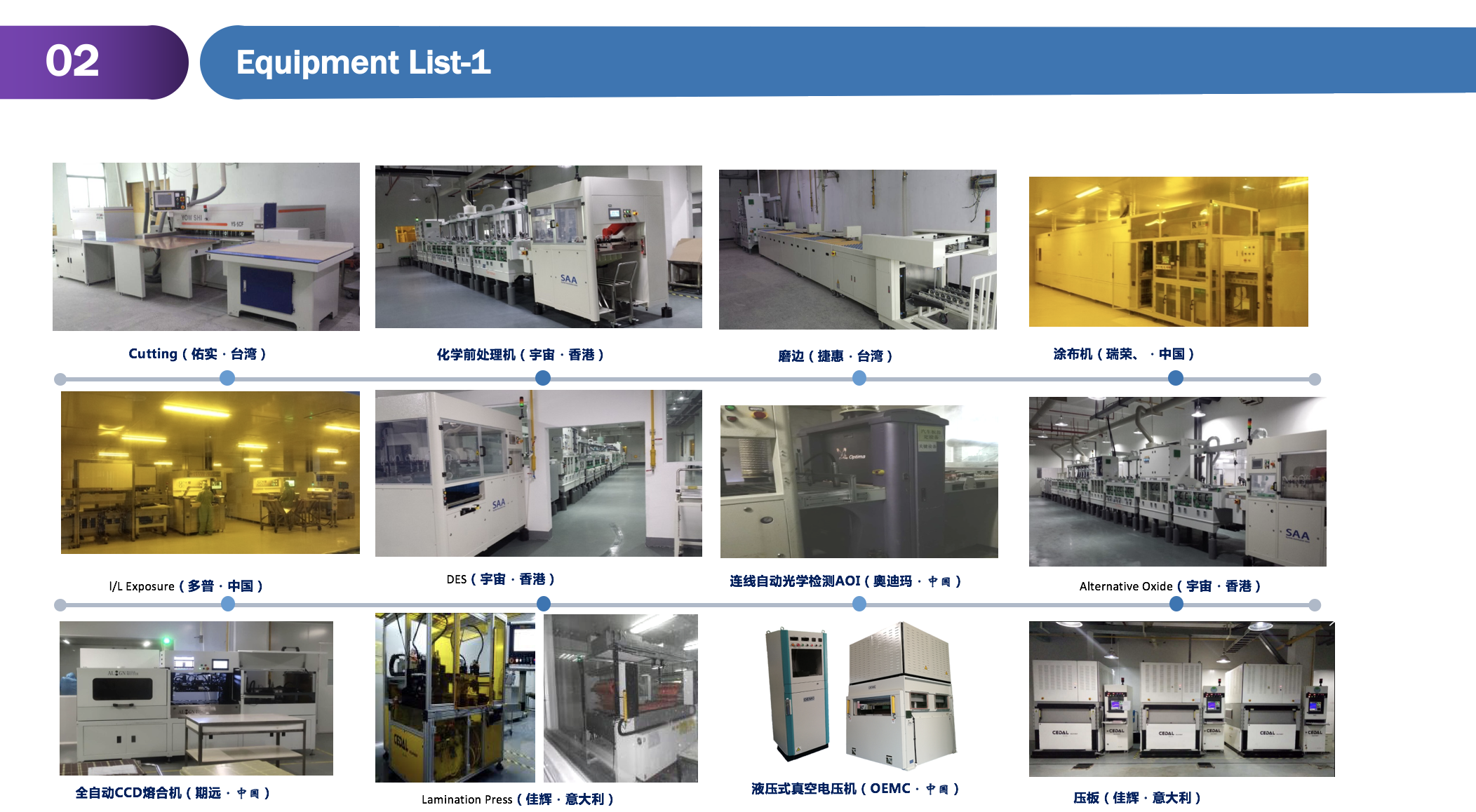
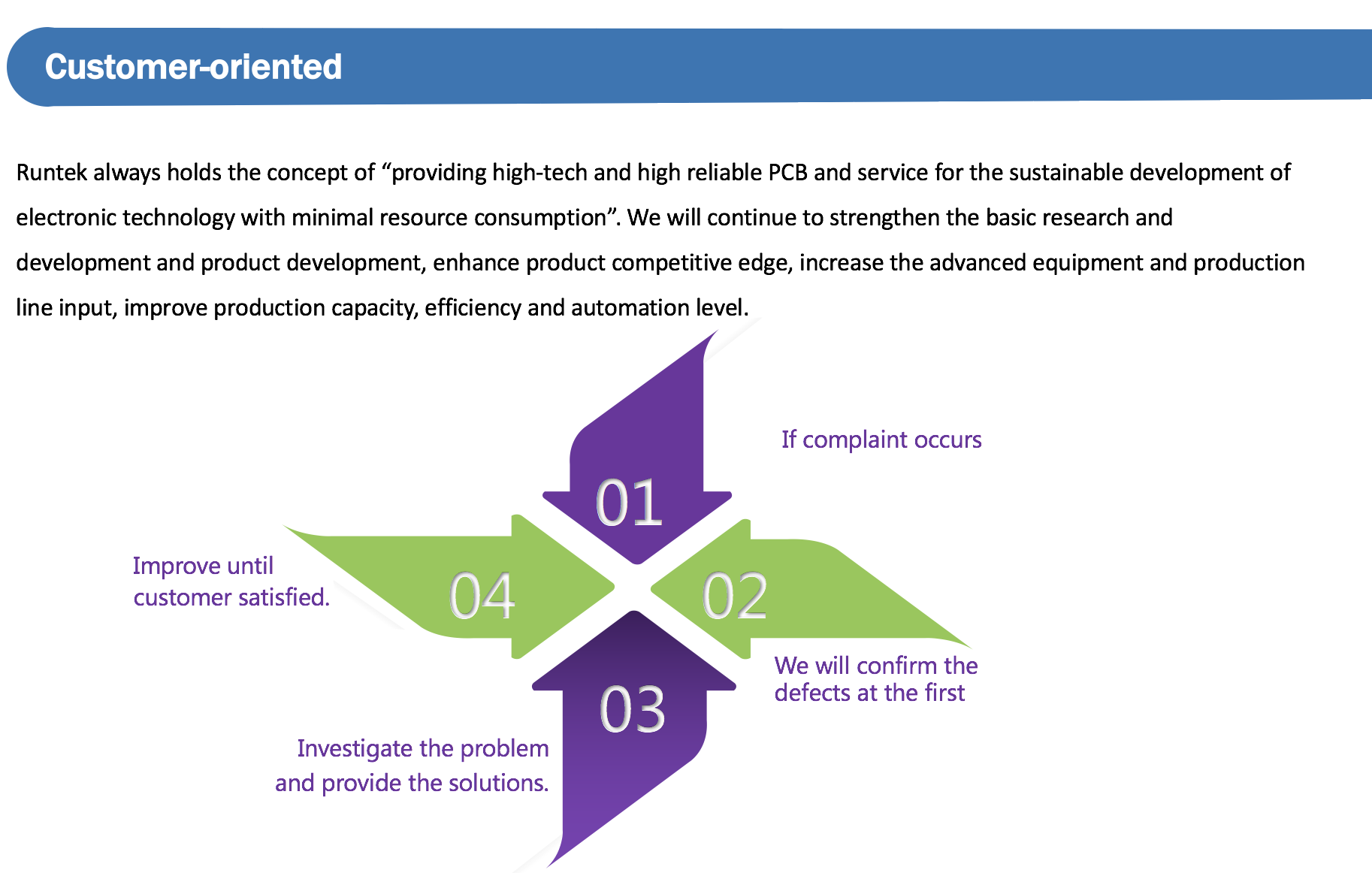
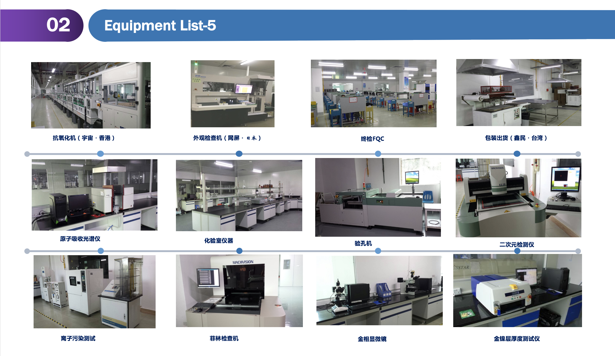
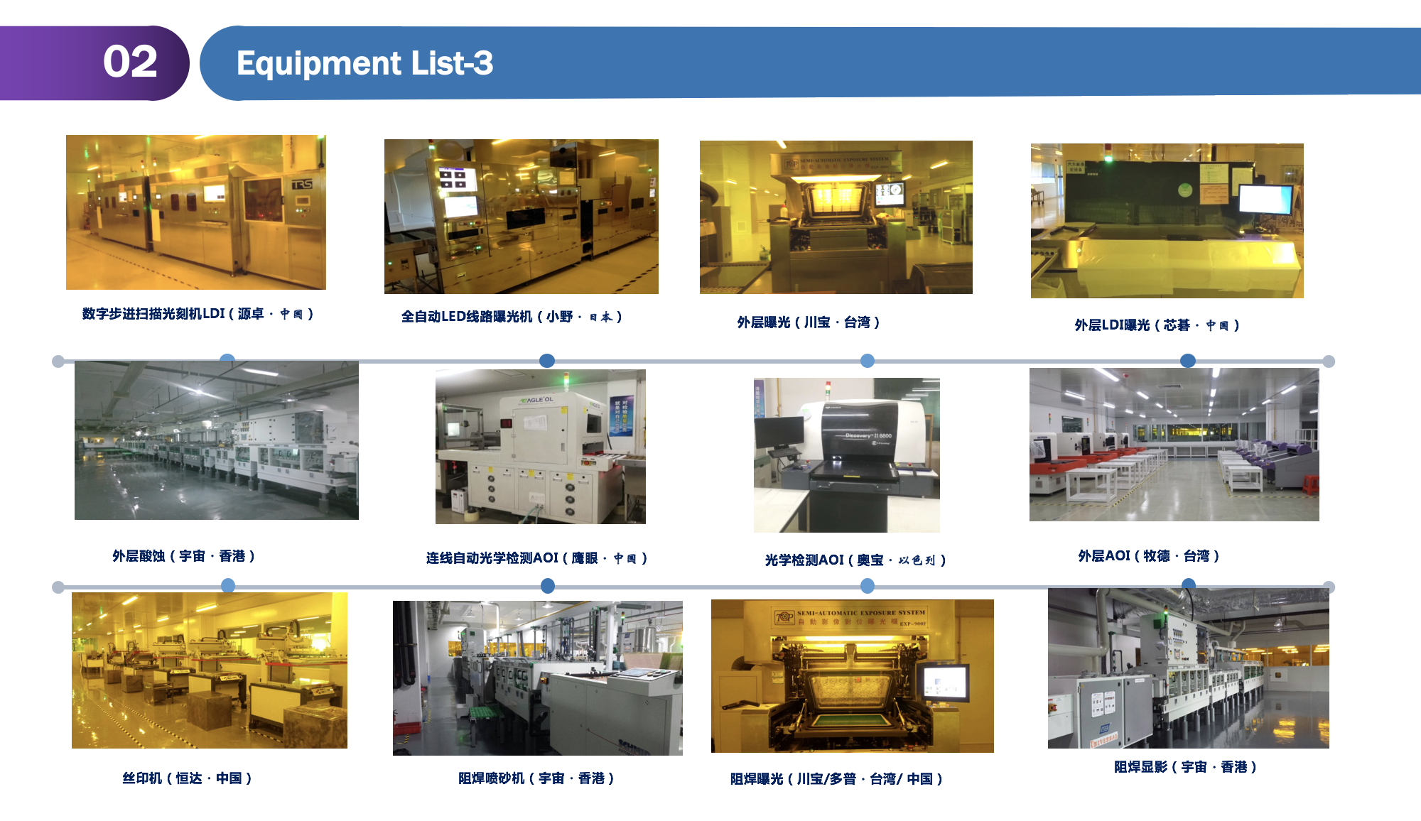
Runtek always holds the concept of “providing high-tech and high reliable PCB and service for the sustainable development of electronic technology with minimal resource consumption”. We continue to strengthen R&D, enhance product competitiveness, and invest in advanced equipment to improve automation, efficiency, and production capacity.

  • Japanese Laser Exposure Machine (25μm resolution)
  • Four Shots per Laser Hole (0.075mm drill diameter)
  • Copper Thickness: 18–30μm for High Reliability
  • Compliant with IPC-2 Standards

Advanced Manufacturing Capabilities

Runtek leverages cutting-edge technology and precision engineering to deliver PCBs that meet the highest standards in performance and reliability.

Laser Drilling

Ultra-Precision Laser Drilling

0.075mm drill diameter with four-laser shots per hole ensures unmatched accuracy and reliability.

High-Density Interconnect

High-Density Interconnect (HDI)

Advanced build-up HDI technology for compact, high-performance electronics in 5G, IoT, and mobile devices.

Heavy Copper PCB

Heavy Copper & Power Boards

Up to 30μm copper thickness for high-current applications in industrial control and power systems.

Impedance Control

Impedance-Controlled PCBs

Precision-controlled signal integrity for high-speed communication and RF applications.

Rigid-Flex & FPC Solutions

Custom flexible and rigid-flex PCBs for space-constrained and high-mobility applications.

Fast Turn Prototyping

Low-cost, fast-turn prototypes under IPC-2 standards — ideal for R&D and product validation.

Our PCB Product Range

Customized, high-reliability PCBs for diverse high-tech industries.

HDI Board

HDI Board

High-Density Interconnect PCBs with microvias, ideal for smartphones, IoT modules, and 5G base stations.

  • • 2+8+2, 2+10+2, 2+14+2 layer stackups
  • • 0.075mm laser microvias
  • • IPC Class 2/3 compliant
HAR Board

HAR Board

High Aspect Ratio PCBs for high-layer-count applications requiring deep drilling precision.

  • • Up to 20+ layers
  • • Aspect ratios up to 12:1
  • • High reliability for industrial systems
VOP Board

VOP Board

Via on Pad technology for compact, high-density routing in advanced HDI designs.

  • • Microvia on pad with filling
  • • Enhanced signal integrity
  • • Ideal for BGA packages
Stamp Board

Stamp Board

Panelized PCBs with stamp-hole breakaway for efficient assembly and handling.

  • • Easy depaneling
  • • Cost-effective for mass production
  • • Compatible with SMT lines
PTH Board

PTH Board

Plated Through-Hole PCBs for mixed-technology assemblies and rugged applications.

  • • Through-hole and SMT compatible
  • • High mechanical strength
  • • Used in power and industrial boards
Impedance Board

Impedance Board

Controlled impedance PCBs for high-speed digital and RF signal transmission.

  • • Single-ended & differential pairs
  • • ±10% impedance tolerance
  • • Used in 5G, optical modules, servers
Custom Rigid-Flex

Rigid-Flex PCB

Hybrid rigid and flexible circuits for compact, dynamic applications.

  • • 2–8 flex layers
  • • High bend cycle endurance
  • • Ideal for medical and aerospace
Heavy Copper PCB

Heavy Copper PCB

High-current power boards with thick copper layers for thermal and electrical performance.

  • • 3oz to 10oz copper
  • • Thermal management optimized
  • • Used in power supplies and EVs

Frequently Asked Questions

What is HDI PCB and why is it important?

HDI (High-Density Interconnect) PCBs use microvias, fine lines, and high layer density to enable smaller, faster, and more reliable electronic devices. They are essential for smartphones, IoT, and 5G technologies.

Can you produce impedance-controlled boards?

Yes, Runtek offers precision impedance-controlled PCBs with tight tolerances, ideal for high-speed digital and RF applications such as servers, optical modules, and 5G base stations.

What materials do you support?

We support FR-4, HF (high-frequency) materials like Rogers, polyimide for flex, and metal-core substrates. Material selection is optimized for frequency, thermal, and mechanical requirements.

What is your lead time for prototypes?

Standard prototype lead time is 5–7 days. Fast-turn options are available. Production lead times vary based on complexity and volume.

Do you offer DFM support?

Yes, our engineering team provides free Design for Manufacturing (DFM) analysis to ensure your design is optimized for yield, reliability, and cost-efficiency.

Get in Touch

You are welcome to visit our factory or share your custom requirements. We respond to all inquiries within 12 hours.

Phone

+86 13681795715

Business Hours

Mon–Fri, 10 AM – 6 PM

Notice for Buyers: If you are a buyer, the above information is generated by AI collection and does not constitute any advice. If necessary, please visit the corresponding official website.

For Domain Owners: If you are the domain owner and do not want to be included by fobcompany.info, please contact [email protected] via your corporate email to cancel. We will cancel your inclusion within 3 business days.

如果您是域名所有者 不想被fobcompany.info收录 请用企业邮箱联系[email protected] 取消收录 我们将在3个工作日取消您的收录

Service Request: If you are other domain and want to be included, please contact [email protected]

如果您是其他域名合作 也请联系[email protected]